Chinese semiconductor thread II

tphuang

General
Staff member
Super Moderator
VIP Professional
Registered Member
TSMC confirmed that it will gradually withdraw from the gallium nitride (GaN)


Please, Log in or Register to view URLs content!

The article is written in a somewhat obfuscated style, but the key points are:

1. TSMC will exit GaN field due to price pressure from Chinese suppliers.

2. Big US customer Navitas will switch to Taiwan Powerchip

3. Big Chinese customer BYD is not clear to where it will go. BYD went with TSMC instead of Chinese leader Innoscience because the latter is also an IDM (sell their own chips) so it is also in some way a competitor of BYD

The Digitimes article frames the exit of TSMC from GaN as a problem for China, but of course this is just cope. It is obvious Chinese GaN suppliers will greatly benefit from this decision by TSMC.
there are so many GaN producers in China that BYD can just go to any of them really.

The issue is that Ga is still allowed to be exported at this amount that Powerchip somehow can be economical. That is terrible export control by China. wtf
 

tokenanalyst

Brigadier
Registered Member

Wanye Enterprise: Subsidiary plans to participate in the establishment of an equity investment fund with RMB 299 million​

Wanye Enterprise issued an announcement stating that according to the company's strategic plan, Nantong Wanye intends to invest in the establishment of Chongqing Liangjiang Industrial Fund as a limited partner with Chongqing Liangjiang New Area High-quality Development Industry Private Equity Investment Fund Partnership (Limited Partnership) (hereinafter referred to as "Chongqing Liangjiang High-quality Industry Fund"). The target fundraising scale of Chongqing Liangjiang Industrial Fund is tentatively set at 1 billion yuan, of which Nantong Wanye intends to subscribe 299 million yuan, accounting for 29.90% of Chongqing Liangjiang Industrial Fund. The source of funds for this investment is Nantong Wanye's own funds.

Wanye Enterprise pointed out that the main investment direction of Chongqing Liangjiang Industrial Fund is integrated circuits and the upstream and downstream of the industrial chain, while taking into account investments in high-quality companies that are in line with national policy orientations and have core technologies and broad market prospects, including but not limited to growth-stage and mature-stage companies in the direction of new-generation information technology and unlisted companies, in fields such as digital economy, artificial intelligence, new energy, etc.

In recent years, Kaishitong has achieved breakthroughs in the field of key semiconductor equipment. Low-energy, large-beam and high-energy ion implanters have been mass-produced and introduced into 12-inch wafer production lines. The cumulative orders have reached 60 units, and more than 40 units have been delivered. The mass-produced wafers have exceeded 5 million pieces, covering the four major fields of logic, storage, CIS and power chips. At the same time, Kaishitong has independently developed and mastered key core technologies, systematically overcome technical difficulties such as injection angle control, particle contamination control, high yield, and high production capacity, and achieved innovative breakthroughs in the localization of key components such as long-life ion sources, high-quality analytical magnets, and beam deceleration devices.

Please, Log in or Register to view URLs content!
 

tokenanalyst

Brigadier
Registered Member

Huawei HiSilicon Cat.1 IoT chip Hi2131 is officially launched​


On July 10, Huawei HiSilicon officially announced that the Hi2131 Cat.1 IoT chip was officially launched on the market. According to reports, the Hi2131 Cat.1 chip uses an ultra-light chip architecture and minimal sleep management, which reduces sleep power consumption to 150uA. Compared with common chips of the same type, the keep-alive power consumption is reduced by more than 30%, and the data transmission power consumption is also reduced by 10%. The significant optimization of power consumption directly translates into a leap in device endurance. This means that the maintenance cycle of shared devices is greatly extended, and user experience and operation and maintenance costs are optimized simultaneously.

In addition, the downlink signal reception performance of Hi2131 is 1dBm higher than that of similar chips on average, giving the device a more powerful "signal capture" capability. In network edge environments such as underground parking lots and elevator shafts, Hi2131 can still provide a more stable communication link, reduce data packet loss and communication interruption, and ensure stable operation of the device. HiSilicon said that the dual breakthroughs of Hi2131, "high performance + low power consumption", have brought qualitative improvements to multiple key IoT scenarios:

Sharing economy: Lower power consumption ensures long-term reliable operation of shared devices such as power banks and bicycles. 1dBm performance gain ensures smooth operation of underground garage equipment and reduces operation and maintenance costs.
Mobile payment: Performance improvements ensure stable signals in crowded exhibitions, remote markets and other places, increasing payment success rates; ultra-low power consumption extends device usage time.

Smart security: 150uA sleep power consumption extends the battery life of wireless cameras, and 1dBm gain ensures that the device is stably online in environments such as elevators and corridor monitoring. HiSilicon also stated that Hi2131 will serve as a key link between the physical world and the digital ecosystem, promoting the popularization of wide-area Internet of Things applications.

Please, Log in or Register to view URLs content!
 

tokenanalyst

Brigadier
Registered Member

Breaking the limitations of the electrical domain! A Chinese team launched the world's first programmable all-optical signal processing chip​


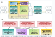
According to scitechdaily, a Chinese research team composed of institutions such as Huazhong University of Science and Technology, Shanghai Jiaotong University, University of Electronic Science and Technology of China and Nankai University has recently successfully developed the world's first programmable single-chip all-optical signal processing (AOSP) chip, which can support optical filtering, signal regeneration and logical operations, breaking the limitation of traditional silicon photonics requiring "optical-electrical-optical (OEO)" conversion, allowing data to maintain the optical signal state from input to output, and moving towards a new high-speed computing architecture that does not require switches.
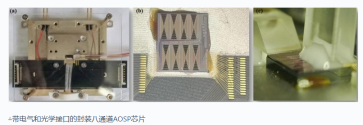
1752245458253.png1752245476446.png

Breakthrough in programmable AOSP chip development
A research team consisting of Professor Zhang Xinliang of Huazhong University of Science and Technology, Professor Su Yikai of Shanghai Jiaotong University, Professor Qiu Kun of University of Electronic Science and Technology of China, and Academician Zhu Ninghua of Nankai University has successfully developed a monolithic integrated programmable all-optical signal processing (AOSP) chip. The chip supports key functions such as optical filtering, signal regeneration, and logic operations. The project originated from a national project aimed at developing silicon-based reconfigurable AOSP technology.

By leveraging the core advantages of silicon photonics, such as CMOS compatibility, minimal signal loss, compact form factor, and strong optical nonlinearities, researchers have produced a chip that can meet the stringent requirements of next-generation optical networks.
These include high-speed data transmission, compatibility with advanced modulation formats, and support for wavelength-transparent operation. The team has experimentally verified the chip's ability to perform dynamic filtering, logic calculations, and signal regeneration, laying a solid foundation for its use in cutting-edge applications such as optical communications, advanced computing, imaging, and sensing.
Overcoming the limitations of silicon photonics
There are several technical barriers to developing a programmable all-optical signal processing (AOSP) platform on silicon-on-insulator (SOI) technology. A major issue is that silicon exhibits carrier-related effects, particularly two-photon absorption (TPA) and free-carrier absorption (FCA), which limit the amount of power available for nonlinear interactions, thereby weakening these effects. In addition, the high refractive index contrast in silicon leads to severe confinement of the optical field, which increases scattering losses, complicates the precise control of light propagation, and introduces significant optical and thermal crosstalk.
To overcome these limitations, researchers have introduced improved fabrication methods, innovative device structures, and novel materials. One key advance involves the development of ultra-low-loss silicon waveguides and high-quality microresonators through enhanced manufacturing techniques. These components enable integrated photonic filters that offer wide, reconfigurable bandwidths and tunable free spectral ranges, allowing highly flexible and precise manipulation of input optical signals.

Chip performance indicators and future prospects
This study highlights key advances in the development of programmable AOSP chips. Through structural and material innovations, key challenges in building large-scale integrated AOSP photonic chips, such as high transmission loss, weak nonlinear effects, limited light field control, and severe optical, electrical, and thermal crosstalk, were addressed. The ultra-low-loss silicon waveguide had a loss as low as 0.17 dB/cm and a Q factor as high as 2.1106.

The research team has achieved advanced integrated filters with bandwidths that can be tuned from 0.55 pm to 648.72 pm (i.e., over three orders of magnitude) and FSRs that can be tuned from 0.06 nm to 1.86 nm (30 times). Absolute FWM conversion efficiencies as high as 12 dB have been demonstrated, which is critical to ensuring the success of high-performance logic and regenerative operations.
An eight-channel multifunctional single-chip integration of filtering, logic, and regeneration has been achieved, integrating 136 devices (including filters, logic gates, regenerators, gratings, MMIs, electrodes, etc.) on a single chip. It has been proven that the total signal processing capability is up to 800 Gb/s (operating at 100 Gb/s per channel), and it can accommodate multiple modulation formats, including DPSK and OOK. A complete set of CLUs has been generated for logic operations, and QPSK regeneration has been proven to improve receiver sensitivity by more than 6dB. By leveraging advanced optoelectronic packaging technology, chip-level routing and processing of multi-channel signals have been verified.

Due to the inherent ultrafast characteristics of optical Kerr nonlinearity (on the femtosecond time scale), these efforts lay the foundation for the design and manufacture of faster large-scale silicon-based AOSP chips. Looking ahead, improvements in nanofabrication technology, new materials, and packaging processes are expected to further improve the performance and flexibility of AOSP chips, providing more efficient optical solutions for high-speed communications and advanced computing, and the optical components on the chip will move from supporting roles to leading roles. If logical operations, data routing, and even memory access can be completed in the optical domain in the future, whether switches are still necessary components will inevitably become the focus of industry discussion.

Please, Log in or Register to view URLs content!
 

tokenanalyst

Brigadier
Registered Member

Shangji Semiconductor Completes C Round of Financing of Hundreds of Millions of Yuan​


Recently, Wuxi High-tech Zone company Shangji Semiconductor completed a C round of financing worth hundreds of millions of yuan. This round of financing was jointly invested by CRRC Guochuang, Wuxi Zhanxin Fund, Nanjing Jushi Suqian Industrial Investment, Huaqiang Venture Capital, Guoxin Hongsheng, Guangzhou Industrial Investment and B round investor Legend Capital. The financing funds will mainly be used to increase research and development efforts and expand production scale.

Shangji Semiconductor is a manufacturer specializing in the research and development and production of domestic semiconductor equipment. Its domestic market share of PVD equipment in the subdivided track is more than 80%. It focuses on the research and development and production in the fields of physical vapor deposition (PVD), chemical vapor deposition (CVD), and plasma dry etching (ETCH). Its main equipment includes metal sputtering deposition, enhanced plasma chemical vapor deposition, plasma dry etching, etc., serving customers in the fields of integrated circuits, power devices, micro-electromechanical systems, and advanced packaging around the world.

Please, Log in or Register to view URLs content!
 

tokenanalyst

Brigadier
Registered Member

Au-Au bonding in MEMS applications

Au-Au bonding (Au-Au bonding/gold-gold bonding) is a common wafer bonding technology in the MEMS field, mainly used to achieve packaging, electrical interconnection or structural connection between micro devices. Due to the excellent conductivity, chemical stability and oxidation resistance of gold, Au-Au bonding has important application value in the manufacture of high-performance and high-reliability MEMS devices.

1752246398440.png

MEMS devices, such as inertial sensors, pressure sensors, and RF MEMS, usually require a vacuum or controlled atmosphere environment to ensure performance. Au-Au bonding has become the preferred process for hermetic packaging due to its excellent sealing and corrosion resistance.

For example, Bosch uses Au-Au bonding in its MEMS accelerometer and gyroscope applications to ensure long-term stable operation of the devices. Au-Au bonding has low resistance, high conductivity and excellent anti-electromigration performance, and is suitable for high-frequency RF MEMS, such as 5G RF filters, millimeter wave antennas, etc. and power MEMS, such as MEMS relays. In CMOS-MEMS integration, Au-Au bonding can achieve wafer-level interconnection, reduce package size and improve signal integrity. Au-Au bonding can withstand high temperatures (>300°C) and mechanical stress, and is suitable for MEMS devices in harsh environments such as automotive electronics, aerospace, etc.

Au-Au bonding cross section

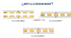
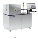
By using the Au-Au bonding recipe of the CFMEE WB 8 wafer bonder, the hot-press bonding process is automatically performed, the bonding time is kept long enough under high temperature and high pressure conditions, and the wafer is removed after cooling to room temperature. After that, the bonded wafer is cut into several 5x5mm chips by a wafer dicing machine. In order to observe the bonding interface under SEM (scanning electron microscope), the chip needs to be processed. The actual bonding effect of the gold-gold hot-press bonding section can be clearly seen in the figure below. The SEM test shows that the gold-gold interface is completely fused and the atomic-level diffusion is sufficient, forming a bonding layer with high mechanical strength and excellent electrical properties, which verifies the good hot-press bonding quality.
1752246411430.png1752246458701.png1752246470624.png


The CFMEE WA 8 wafer aligner supports sub-micron alignment and is suitable for precision bonding of MEMS devices. The WA 8 wafer aligner is equipped with an optical alignment system to ensure accurate matching of the gold layer pattern to reduce the offset after alignment. After the fixture loaded with the aligned wafer stack is moved into the CFMEE WB 8 wafer bonder, the thermal compression bonding process is performed, and the offset after bonding is stably controlled within 6 microns (gold-gold diffusion bonding process).

Au-Au bonding usually requires high temperature (200-400°C) and high pressure (10-100kN). The CFMEE WB 8 bonder adopts a modular design and supports adjustable temperature control and pressure uniformity (±1%). The bonding system provides a bonding force of up to 100kN, which is suitable for hot compression bonding processes of 4/6/8-inch wafers. The longer bonding time of Au-Au bonding requires extremely high high pressure and high temperature stability of the equipment to ensure the bonding quality, which can be achieved by using the CFMEE WB 8 wafer bonding equipment. In addition, CFMEE WB 8 supports high vacuum or inert gas environment to improve bonding quality, which can be applied to MEMS devices that require vacuum packaging.

Please, Log in or Register to view URLs content!
 

tokenanalyst

Brigadier
Registered Member

Actinic defect inspection and characterization for extreme ultraviolet mask blanks.​

School of Physics, Changchun University of Science and Technology

Abstract​

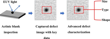
Extreme ultraviolet (EUV) lithography is crucial for advanced semiconductor manufacturing, relying on sophisticated mask technology to transfer intricate patterns onto silicon wafers. The integrity of the EUV mask blanks is essential for producing high-quality masks and semiconductor devices. However, defects in mask blanks, particularly multilayer phase defects, can significantly degrade lithographic quality, affecting device yield and performance. Actinic blank inspection (ABI) has emerged as the most effective strategy for evaluating the initial quality of EUV mask blanks and identifying defects that may compromise the wafer integrity. Additionally, defect characterization helps determine the nature of the defect, its printability, and its potential for repair. This review surveys recent advancements in ABI and defect characterization, covering a range of methodologies, commercial inspection tools and related research efforts that aimed at improving the detection and characterization of multilayer defects.​

1752248262918.png

Please, Log in or Register to view URLs content!
 

tokenanalyst

Brigadier
Registered Member
Precision tool manufacturer Zolix is marketing their Active Vibration Systems for lithography machines.

Nanoscale Guardians of Semiconductor Manufacturing: Active Vibration Isolation Platform Technology​


How environmental vibration affects chip yield and systematic solutions

The semiconductor manufacturing industry has extreme requirements for vibration. As chip manufacturing enters the 3nm era, environmental vibration control has become a core factor in determining the success or failure of the process.

1. Physical limits of process precision

Lithography precision requirements: EUV lithography machines need to draw 5nm line width on silicon wafers (equivalent to one ten-thousandth of a hair), and the platform vibration displacement must be <1nm RMS.

International standard level: SEMIS2/S8 stipulates that key areas must meet VC-E vibration standards (vibration speed in the 1-80Hz frequency band <3μm/s).

ProcessAllowable vibration speed (μm/s)Equivalent displacement (nm) |
EUV lithography≤1.5<0.8
Electron beam testing≤2.0<1.2
Atomic Layer Deposition (ALD)≤3.0<2.0
Wafer dicing≤6.0<5.0
Table 1 Vibration requirements for process steps

Note: Data source: 2023 SEMI International Standard Revision

2. The fatal impact of vibration on semiconductor manufacturing

2.1 Process failure


Due to the influence of the factory environment, the interference from the ground and other vibration sources will directly affect the accuracy of the equipment from a physical level, resulting in the following consequences

Lithography distortion: 1Hz/10nm vibration causes EUV laser interference fringes to shift, causing line width fluctuations exceeding ±15%

Overlay deviation: 3Hz vibration causes a 12-inch wafer to tilt by 0.5μrad, resulting in an inter-layer alignment error of ≥3nm.

Film defects: 5Hz vibration in the CVD process causes airflow disturbance, resulting in film thickness non-uniformity exceeding ±8%

2.2 Economic Losses

In addition to the physical impact, the most direct impact is the economic loss caused by the reduction of yield.

Measured data from a 5nm wafer fab: When the 2-5Hz vibration exceeds the standard by 3dB, the yield rate drops by 1.8%, 1,200 wafers are lost, and the annual economic loss exceeds $25M

3. Systematic Vibration Solutions

3.1. Active vibration isolation system

Core configuration: active vibration isolator.

1752264147565.png

Please, Log in or Register to view URLs content!
 

sunnymaxi

Major
Registered Member
Precision tool manufacturer Zolix is marketing their Active Vibration Systems for lithography machines.

Nanoscale Guardians of Semiconductor Manufacturing: Active Vibration Isolation Platform Technology​


How environmental vibration affects chip yield and systematic solutions

The semiconductor manufacturing industry has extreme requirements for vibration. As chip manufacturing enters the 3nm era, environmental vibration control has become a core factor in determining the success or failure of the process.

1. Physical limits of process precision

Lithography precision requirements: EUV lithography machines need to draw 5nm line width on silicon wafers (equivalent to one ten-thousandth of a hair), and the platform vibration displacement must be <1nm RMS.

International standard level: SEMIS2/S8 stipulates that key areas must meet VC-E vibration standards (vibration speed in the 1-80Hz frequency band <3μm/s).

ProcessAllowable vibration speed (μm/s)Equivalent displacement (nm) |
EUV lithography≤1.5<0.8
Electron beam testing≤2.0<1.2
Atomic Layer Deposition (ALD)≤3.0<2.0
Wafer dicing≤6.0<5.0
Table 1 Vibration requirements for process steps

Note: Data source: 2023 SEMI International Standard Revision

2. The fatal impact of vibration on semiconductor manufacturing

2.1 Process failure


Due to the influence of the factory environment, the interference from the ground and other vibration sources will directly affect the accuracy of the equipment from a physical level, resulting in the following consequences

Lithography distortion: 1Hz/10nm vibration causes EUV laser interference fringes to shift, causing line width fluctuations exceeding ±15%

Overlay deviation: 3Hz vibration causes a 12-inch wafer to tilt by 0.5μrad, resulting in an inter-layer alignment error of ≥3nm.

Film defects: 5Hz vibration in the CVD process causes airflow disturbance, resulting in film thickness non-uniformity exceeding ±8%

2.2 Economic Losses

In addition to the physical impact, the most direct impact is the economic loss caused by the reduction of yield.

Measured data from a 5nm wafer fab: When the 2-5Hz vibration exceeds the standard by 3dB, the yield rate drops by 1.8%, 1,200 wafers are lost, and the annual economic loss exceeds $25M

3. Systematic Vibration Solutions

3.1. Active vibration isolation system

Core configuration: active vibration isolator.

View attachment 155993

Please, Log in or Register to view URLs content!
Chinese suppliers now openly advertising their Lithography subsystems. huge development

first Ultra precision Lithography lens now this Active Vibration System
 
Top