Chinese semiconductor thread II

tphuang

Lieutenant General
Staff member
Super Moderator
VIP Professional
Registered Member
oFilm is in charge of camera modules on phones

Please, Log in or Register to view URLs content!

Recently disclosed to the outside world that floating macro modules, periscope telephoto macro modules, chip anti-shake, variable aperture and telescopic modules have all achieved mass production.

Looks like the domestic phone camera module supply chain is almost complete

looking at oFilm here
Please, Log in or Register to view URLs content!

16.8B in revenue
12.2B in phone
1.9B in EVs
2.4B in new areas

so for camera module companies, vast majority of their revenue comes from phones
 
Last edited:

tokenanalyst

Brigadier
Registered Member
It's a bit disturbing reading this from knowledgeable members. What's the reason for this pessimistic timeline? We know CIOMP has either already completed its LPP prototype or will this year. Unlike SMEE's DUVi stuck in "verification", there isn't an alternative source of EUV lithography machines domestic fabs would rather have. It's not CIOMP's EUV or ASML's like the case with DUVi, it's CIOMP or nothing.

I don't think the SMEE DUVi case should be used as a model for EUV adoption.
SMEE DUVi scanners is already pass the verification stage, those scanners are already patterning wafers. The EUV scanner is probably going to happen sooner than given the resources that Chinese research institution are putting into it.
 

tphuang

Lieutenant General
Staff member
Super Moderator
VIP Professional
Registered Member
Please, Log in or Register to view URLs content!

China's first GaN semi laser chip production line has gone into production at 飓芯科技

Also Xiner semiconductor's new hefei high end power chip packaging base has been completed
Xiner already produces 1200V SIC MOSFT IPM. Looks like they sell wide variety of energy transition chip product
 

tphuang

Lieutenant General
Staff member
Super Moderator
VIP Professional
Registered Member
Please, Log in or Register to view URLs content!

smartsens have launched 17 CMOS chips since 2020 and now has 5.7% of global market share, 5th largest in the world. It now has a line of 50MP main CMOS chip products.

It is now getting into higher end CMOS market, so more options for domestic flagship phones.

GalaxyCore is the other CMOS maker
 

tokenanalyst

Brigadier
Registered Member

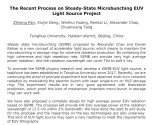
Identification of key aberrations that affect pattern imaging in EUVL.​

Institute of Microelectronics (China)

Abstract​

In EUVL, aberrations play a crucial role in critical dimension (CD) and pattern shift (PS) errors. It is significant to decide aberration compensation and optimization strategies for compensating exposure errors. The modeling process of aberration is time-consuming, mainly because of the need to consider numerous aberrations. In order to save the runtime for aberration modeling, this paper proposes a methodology for identifying the key aberrations that have significant impacts on imaging results. Three different techniques are employed and compared, including single parameter sensitivity analysis, definitive screening design (DSD) method, and SOBOL method that consider the coupling effects of different orders. By comparing the deviations between the imaging results considering only key aberrations and all aberrations, it is found that the identified aberrations achieve extremely high accuracy for various patterns and illumination conditions. Even though the proportion of key aberrations among all aberrations is only a small fraction. All the three methods can achieve that the average CD and PS deviations do not surpass 1%, using 40% of the total 37 aberration items. Thereby, the feasibility of using identified key aberrations for aberration modeling is validated. In addition, we also compare the accuracies of three techniques under the same conditions and found that the SOBOL method is the most suitable technique for identifying key aberrations. Consequently, for specific illumination conditions and corresponding layout patterns, the use of key aberrations is an effective way to characterize the impacts of all 37 aberrations, accelerating the aberration compensation and optimization without sacrificing accuracy.​

Please, Log in or Register to view URLs content!
 

JPaladin32

Just Hatched
Registered Member
This isn't exactly true. Intel's fab in Ireland can produce 4nm chips. Currently Intel does not have enough production to produce a lot at the fab though. So they are sourcing some chiplets from TSMC and others from their own fabs.
Please, Log in or Register to view URLs content!
"Intel 4" and 4nm may be different things. Intel 4 transistor density and transistor dimensions are worse than TSMC 5nm, so the gap between SMIC 7nm and Intel 4 may not be as large as 7nm vs. 4nm suggests.
 

zbb

Junior Member
Registered Member
This isn't exactly true. Intel's fab in Ireland can produce 4nm chips. Currently Intel does not have enough production to produce a lot at the fab though. So they are sourcing some chiplets from TSMC and others from their own fabs.
Please, Log in or Register to view URLs content!

"Intel 4" and 4nm may be different things. Intel 4 transistor density and transistor dimensions are worse than TSMC 5nm, so the gap between SMIC 7nm and Intel 4 may not be as large as 7nm vs. 4nm suggests.

The most advanced node in production in the US is the "Intel 4", which is a marketing term meant to sound like it's equivalent to 4nm process. However, transistor density for "Intel 4" is much lower than TSMC 5nm. In fact, "Intel 4" transistor density is closer to TSMC and SMIC's best 7nm processes than to TSMC's 5nm process. If SMIC 5nm can come close to TSMC 5nm, then they would be ahead of "Intel 4" in terms of transistor density.

Please, Log in or Register to view URLs content!

Intel 4TSMC 5nmTSMC 7nm (N7+)SMIC 7nm (N+2)
123.4138.2113.9113.6
 
Top