Chinese semiconductor industry

Status
Not open for further replies.

tokenanalyst

Brigadier
Registered Member

Wafer Inspection​

Wafer is the most basic semiconductor material for making IC, and the quality of wafer will directly determine the quality of IC finished product. Due to different process levels, wafers may have three types of defects: redundancy, crystal defects and mechanical damage during the production stage. Wafer inspection equipment is mainly aimed at the appearance inspection of wafers after cutting, such as: size, damage, cracks, pores, cracks, poor nickel layer, etc. Therefore, efficient and accurate inspection equipment is the guarantee of providing high-reliability wafer materials. Compared with traditional manual inspection, machine vision inspection has the advantages of high precision, high efficiency, continuity, and non-contact avoidance of pollution.

Please, Log in or Register to view URLs content!
independently developed by Hibson Technology , the detection is not limited by the material, and can effectively solve the detection of reflective/transparent objects. 3D line spectral confocal sensor, through non-contact detection, the scanning rate can reach 35,000 lines/second, and the ultra-high repeatability of ±0.1μm, suitable for high-precision Z-axis positioning of patterned wafers and other scenarios.
Please, Log in or Register to view URLs content!
can also achieve high-precision thickness measurement applications by supporting a double-head bracket.

Please, Log in or Register to view URLs content!


Please, Log in or Register to view URLs content!

Sensors for wafer optical metrology equipment.
 

tokenanalyst

Brigadier
Registered Member

Novel Through Glass Via Technology Developed for 3D Advanced Packaging​

Editor: ZHANG Nannan | Jun 16, 2022
Please, Log in or Register to view URLs content!

Please, Log in or Register to view URLs content!
of the Chinese Academy of Sciences (CAS) has developed Through Glass Via (TGV) process for three dimensional (3D) advanced packaging, enabling low transmission loss and high vacuum wafer-level packaging of high-frequency chips and Microelectro Mechanical Systems (MEMS) sensors.
3D packaging technology has become one of the main driving forces for the development of integrated circuits. TGV is a new vertical interconnection technology applied in wafer-level vacuum packaging. It has good electrical, thermal and mechanical properties, and achieves interconnection with the shortest distance and the minimum spacing between chips.
"We have overcome technical problems such as the manufacture of high-uniformity glass micropore arrays, glass dense reflow, and high-density filling of glass micropores and metals," said Dr. LI Shan, who conducted the research.
The researchers proposed a new TGV wafer manufacturing scheme. The newly-developed TGV wafers boasted high uniformity, high density and high aspect ratio, which enabled ultra-low leakage rate and ultra-low signal loss. After testing, they found that some parameters were even better than international standards.
"They can be applied to 5G/6G high-frequency chips such as ring resonators, waveguide slot antennas, millimeter-wave antennas, as well as new 3D packaging requirements for MEMS gyroscopes and accelerometers." said Dr. LI Shan, "and we can make different sizes according to requirements."
Related technologies have been supported by projects from the National Natural Science Foundation of China, the Ministry of Science and Technology, CAS, and Anhui Province.​
W020220616604398612608.jpg

Figure 1. Conductive metal-based TGV wafers. (Image by HFIPS)
W020220616604399198396.jpg

Figure 2. Conductive silicon-based TGV wafers. (Image by HFIPS)

Please, Log in or Register to view URLs content!
 

Strangelove

Colonel
Registered Member
Please, Log in or Register to view URLs content!

Mainland chipmakers among world's top 10​


62ba51d1a310fd2bec92387d.jpeg
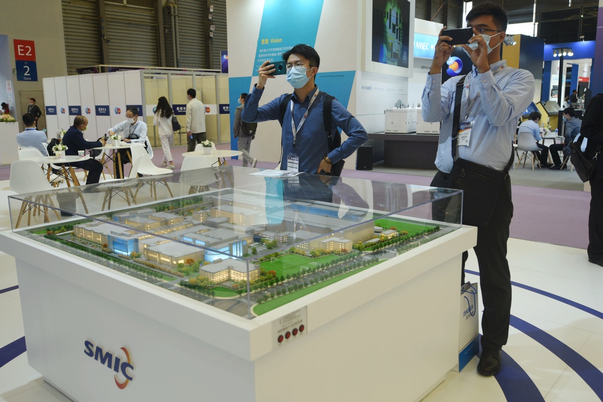
The booth of Semiconductor Manufacturing International Corp during an expo in Shanghai.LONG WEI/FOR CHINA DAILY
SMIC, HuaHong and Nexchip promise supply chain security

The Chinese mainland is making fresh progress in manufacturing semiconductors.

For the first time, three Chinese mainland chipmakers accounted for more than 10 percent of the global foundry revenue in the first quarter of this year, a new report has stated.

Foundry is industry parlance for contract chipmaking. Data from TrendForce, a market research and intelligence provider, showed China's Semiconductor Manufacturing International Corp ranked fifth among the top 10 global foundry revenue earners in the January-March quarter, with a market share of 5.6 percent.

Shanghai-based HuaHong Group, another major Chinese semiconductor maker, ranked sixth with a market share of 3.2 percent.

Nexchip, based in Hefei, Anhui province, took ninth place, with a market share of 1.4 percent.

"Although demand for consumer electronics remains weak, structural demand growth in the semiconductor industry, including for servers, high-performance computing, automotive and industrial equipment, has not flagged, becoming a key driver for medium- and long-term foundry growth," TrendForce said.

At the same time, due to robust wafer production at higher pricing in the first quarter, quarterly output value reached $31.96 billion, up 8.2 percent quarter-on-quarter, a new high for the 11th consecutive quarter. The rise, however, was marginally less than that seen in the previous quarter.

In terms of ranking, the biggest highlight is that Nexchip surpassed Tower, an Israeli chip company acquired by Intel, for the ninth position, TrendForce said.

The progress came as Chinese mainland chip companies are making a bigger push to accelerate development after the United States government imposed sanctions on a string of local tech heavyweights such as Huawei Technologies Co.

Nineteen of the world's 20 fastest-growing chip industry firms over the past four quarters, on average, are from the Chinese mainland, according to data compiled by Bloomberg. That compared with just eight firms at the same point in time last year.

Xiang Ligang, director-general of the Information Consumption Alliance, a telecom industry association, said the Chinese mainland companies have realized the importance of safeguarding supply chain security. And amid uncertainties, they have also become more eager to cultivate a range of suppliers.

That is not all. The Chinese mainland chipmakers are increasingly relying on domestic suppliers of crucial components.

The Chinese mainland accounted for 11 percent of worldwide semiconductor fabrication capacity in 2019, and the number is forecast to reach 18 percent in 2025 and nearly 19 percent in 2030, according to the Semiconductor Industry Association, a Washington-based group that represents the US semiconductor industry.

Roger Sheng, vice-president of research at Gartner, a market research firm, said as the world's largest chip market, the Chinese mainland has made tremendous progress in developing its semiconductor industry in recent years.

But there is still a big technical gap between local chipmakers and their foreign peers, especially in high-end chipmaking equipment and fundamental chip materials, Sheng said.

The Chinese mainland, for instance, relies heavily on import of lithography machines that play a crucial role in chip production.

To achieve breakthroughs in these areas, money is not enough. "Talent and time are key," Sheng said.

In 2021, for the first time, the sales revenue of the integrated circuit or IC industry in the Chinese mainland exceeded 1 trillion yuan ($157.3 billion), up 18 percent year-on-year, the China Semiconductor Industry Association said.

In comparison, global semiconductor revenue grew at a compound annual growth rate of 25.6 percent to $552.9 billion last year.
 

gelgoog

Brigadier
Registered Member
So this all seems fantastic and really good news for anyone hoping for China closing the gap being denied equipment from ASLM and other companies by the US - ironically the embracer of market competition. For myself, with very limited knowledge in this field but still interested in Chinese success, I would like to hear what people on this thread think it will take until China reach the TSMC and leading edge technology in an industrial level. I use to say to my friends that in 5 year China has closed the gap. What is realistic according to You?
It is all dependent on access to tools and materials. SMIC was basically just a couple generations behind TSMC until the US sanctions on EUV tools hit. SMIC had already done research on the processes to have parity with TSMC but without the tools and materials they can't produce anything with those processes. Chinese industry is working on making their own EUV tools and materials but I doubt it will happen before end of decade and then this process will start all over again. At the same time it isn't like TSMC is standing still. TSMC is basically introducing 4nm this year and 3nm soon with 2nm on roadmap where 2nm is first node with GAA transistors.
 

hvpc

Junior Member
Registered Member
Please, Log in or Register to view URLs content!

Mainland chipmakers among world's top 10​

For the first time, three Chinese mainland chipmakers accounted for more than 10 percent of the global foundry revenue in the first quarter of this year, a new report has stated.
This claim could be interpreted incorrectly. China foundries had over 10% share back in ~2008. But 2022Q1 is the first time "three chipmakers" combined for >10% (back in 2008 it took more than three chipmakers to crack 10% before).

For those are big on rankings/stats, this is the ranking that the article referenced:

20220620_151614_0620_sr-1q22晶圓代排名.png
 
Last edited:

mossen

Junior Member
Registered Member
Chinese industry is working on making their own EUV tools and materials but I doubt it will happen before end of decade and then this process will start all over again. At the same time it isn't like TSMC is standing still. TSMC is basically introducing 4nm this year and 3nm soon with 2nm on roadmap where 2nm is first node with GAA transistors.
New nodes are becoming more and more inefficient. AMD publicly said that upcoming GPUs will require more and more power for this reason. As a result, I suspect it will be easier to catch up once China has the tools because inefficiency is increasing at the frontier.
 

ansy1968

Brigadier
Registered Member
New nodes are becoming more and more inefficient. AMD publicly said that upcoming GPUs will require more and more power for this reason. As a result, I suspect it will be easier to catch up once China has the tools because inefficiency is increasing at the frontier.
@mossen bro I'll repost an article from Semiconductor Engineering by Mark Lapedus on EUVL, hope @hvpc @latenlazy @tokenanalyst @FairAndUnbiased @krautmeister @PopularScience and other experts can expound on this.

Please, Log in or Register to view URLs content!

What’s Next In Fab Tool Technologies?​

594Shares
facebook sharing button
36
twitter sharing button
46
linkedin sharing button
504
sharethis sharing button


MAY 12TH, 2021 - BY:
Please, Log in or Register to view URLs content!

popularity

Experts at the Table: Semiconductor Engineering sat down to discuss extreme ultraviolet (EUV) lithography and other next-generation fab technologies with Jerry Chen, head of global business development for manufacturing & industrials at Nvidia; David Fried, vice president of computational products at Lam Research; Mark Shirey, vice president of marketing and applications at KLA; and Aki Fujimura, CEO of D2S. What follows are excerpts of that conversation. To view part one of this discussion, click
Please, Log in or Register to view URLs content!
. Part two is
Please, Log in or Register to view URLs content!
.

SE: EUV lithography is in production at the 7nm and 5nm logic nodes. We’ve heard some chipmakers are moving from EUV single patterning to EUV double patterning at 5nm and beyond. From there, we’re expecting to see high-NA EUV, which is in R&D. What are you seeing from your vantage point here?
Fried
: If EUV had been deployed on its originally-slated schedule several years earlier, it would have been used as a single patterning scaling replacement and as a stepwise progression from 193nm immersion lithography. Unfortunately, it took longer than expected to get EUV established. This created a continuing need for multiple patterning with 193nm immersion, which includes self-aligned double patterning and self-aligned quad patterning. I worked on some early double-patterning initiatives using a 90nm reticle about 20 years ago, when self-aligned double patterning wasn’t truly viable. At the time, these efforts used a little trick that we played in the lab. Due to EUV taking so long to come to fruition, we built a much more robust version of double-patterning and quad-patterning to fill the void left by the lack of commercial EUV capabilities. EUV is now finally available, but it has come at a time when it can’t just be used as a single-patterning replacement. In several applications, EUV will most likely be deployed as the litho replacement during the litho step in double patterning. EUV still provides a huge advantage, since it will eliminate significant process time and complexity. Usually, these types of lithography scaling changes come with material challenges. I lived through the 248nm to 193nm lithography transition, and it was a difficult transition because many of the materials weren’t fully ready for manufacturing criteria. The equipment at the time was ahead of the materials. With EUV, it’s a little bit different. The equipment took so long to arrive and due to the extremely short wavelength, EUV introduced several unique material challenges. In addition, any stepwise progression in the fab has ripple effects into every other aspect of the fab. However, I believe there are adequate levels of innovation in all semiconductor fabrication sectors to support the progression to EUV along with the next big stepwise progressions.
Shirey: There is a tremendous amount of work being done across these generations of EUV. Starting with EUV reticles, there are inspection strategies being developed and deployed from initial qualification in the mask house to reticle re-qualification in the fab. As we try to squeeze more out of the current EUV systems, there is continuous development with resists and increases in source power that drive inspection and metrology characterization projects. There is ongoing work to optimize litho and etch inspection steps for EUV defects like stochastic defects in development and high-volume manufacturing.
Fujimura: High-NA is a clever invention. But the mask infrastructure needs to be shared between 193i and EUV, including high-NA. So in order for high-NA to be viable and attain a higher-numerical aperture, high-NA EUV uses 8:1 ratio of mask sizes to wafer sizes in one dimension while retaining the traditional 4:1 ratio in the other dimension. While EUV masks are substantially different in being reflective masks, mask sizes are the same for both. High-NA allows you to preserve that by deciding to split what used to be a full reticle design into two reticles. Each feature on a mask now reflects twice as much EUV energy off the reticle, improving the ability to write smaller features more precisely and reliably. Of course, 8:1 in both dimensions would be even higher NA. But that would either reduce the throughput of wafer manufacturing by 4X instead of just 2X. Or, it requires an entirely new mask infrastructure that handles much bigger masks, while also continuing to support the traditional sizes. High-NA will bring about opportunities to improve software processing infrastructure like inverse lithography technology (ILT) for wafer lithography and mask process correction (MPC) for mask writing.
SE: What are some of the new and enabling fab technologies on the horizon?
Fried
: Lam has been public with a dry resist solution, which enables height scaling for depth of focus, high absorption and collapse margin. And that is a massive innovation that goes alongside EUV. There’s going to be all sorts of new innovations that go with that.
Chen: I’d highlight two technologies that we’re looking forward to now and in the future, both as a consumer of these technologies, and also as a contributor. First of all, as a fabless company, we’re concerned about the lithography challenges facing our foundry partners at leading-edge process nodes. Secondly, process control is becoming increasingly difficult because detecting sub-nanoscale defects is incredibly challenging. In both cases, we’re seeing good results with computational and AI-driven approaches. For example, we’re seeing the adoption of computational lithography used in conjunction with AI to optimize photomasks for yield. We’re also seeing AI being adopted to augment perception for defect inspection and metrology.
Shirey: More chip complexity and semiconductor demand are driving a lot of innovations in inspection and metrology. Some of the key inflections are EUV, nanosheets, advanced memory and automotive electronics. There is innovation happening for EUV reticle pattern quality monitoring for the very tightest leading nodes. Nanosheet and advanced memory are driving the need for inspection and measurement of buried structures, and there are continued innovations with optical and e-beam techniques as well as new technologies like X-ray metrology. At the leading edge there is an insatiable demand for higher capture rates of small defects, so there is continued innovation in light sources, sensors, and algorithms to ensure that inspection and metrology tools detect and measure smaller issues. With increasing silicon content in automobiles, there is innovation to inspect and measure for higher coverage screening applications with analytics to flag potential latent defects that could appear in the lifetime of the chip.
 

ansy1968

Brigadier
Registered Member
continue.....


Fujimura: There are difficulties in going down to even narrower and smaller features. EUV double patterning will certainly be required. But even beyond that, we want to scale even more so that we can build a 20,000 core Nvidia GPU, for example. In order to accomplish that, we need the maximum amount of resilience to manufacturing variation on wafers, and therefore also on masks. Making a very small contact hole resilient to manufacturing variation is a key. If you just want the average of these structures to look okay, that’s not so bad. But in wafer and mask manufacturing, you need all of them to look okay. You need the worst-case examples to look okay. And that’s a really hard thing to do, particularly for lithography at these tiny dimensions. Any help that you can give it is a good thing. One of the ideas that was originally introduced by Luminescent many years ago is curvilinear ILT or inverse lithography technology. This is where you take advantage of curvilinear shapes on the mask to be able to produce a wafer that is more resilient to manufacturing variation. Even though we’ve known that curvilinear ILT shapes on a mask would improve resilience to manufacturing variation on the wafer, we couldn’t do it. The mask infrastructure couldn’t produce curvilinear shapes.
SE: The industry has removed some of the barriers to enable ILT curvilinear masks, right?
Fujimura
: The first barrier, which has been removed, is multi-beam mask writing. In multi-beam mask writing, masks are written with pixel doses instead of individual rectangles or triangles. Multi-beam mask writers write masks at the same speed regardless of the complexity of the shape. The traditional variable-shaped beam (VSB) writers took too long to write curvilinear ILT shapes. But with multi-beam writing, curvilinear masks take the same time as masks that contain only Manhattan geometries. The second thing that happened was the use of GPU acceleration for mask data preparation and also for ILT that outputs the desired mask shapes. All of this allows a pixel-based software algorithm running on a GPU that processes, manipulates, and corrects mask or wafer shapes to process curvilinear shapes efficiently. So multi-beam writing and GPUs together enabled curvilinear mask shapes, both by processing pixels of identical size laid out in a grid, rather than by processing arbitrary rectangles or triangles. In the eBeam Initiative survey, an overwhelming majority of the industry luminaries believe that by 2023, we will be seeing a large number of curvilinear mask shapes on production masks.

Related Stories

Please, Log in or Register to view URLs content!


Next-gen litho is important for scaling, but it’s also expensive and potentially risky.
Please, Log in or Register to view URLs content!

Please, Log in or Register to view URLs content!


New materials and equipment could have a significant impact on both cost and speed.
Please, Log in or Register to view URLs content!

Please, Log in or Register to view URLs content!


How dry resist can overcome challenges at 5nm and below.

Please, Log in or Register to view URLs content!


New tools utilize different approaches, including ML, to boost performance.

Please, Log in or Register to view URLs content!


Why future nodes will require new equipment and approaches.

Please, Log in or Register to view URLs content!


Why this technology is vital for chip scaling, and what problems still need to be resolved.
 

escobar

Brigadier
China currently has few allies and little hope in its fight for silicon supremacy. Even its own consumers and chip designers are reasonably content with reliance on international suppliers. Pushing broader controls will ultimately push Chinese and foreign businesses to develop an alternative semiconductor supply chain, to the benefit of China’s quest to escape technological dependency on the United States.
Please, Log in or Register to view URLs content!
 
Status
Not open for further replies.
Top